About me

I am Boyang Cheng, I received the B.S. degree in Southeast University, Nanjing, China, in 2020. I am currently pursuing the Ph.D. degree in Electrical Engineering at the University of Notre Dame. My research lies at the intersection of digital and analog/mixed-signal circuit design, with a focus on developing energy-efficient and explainable/trustworthy hardware systems. In 2024, I interned at Samsung working on SRAM design, and in 2025, I focused on design technology co-optimization (DTCO).

With a background in both digital and analog/mixed-signal design, I enjoy tackling challenges that require cross-domain thinking and collaboration. My long-term goal is to advance hardware platforms that empower the next generation of intelligent, reliable, and resource-efficient technologies.

Fun Fact: I am the first student of my advisor.

What i'm doing

  • PUF icon

    Hardware Security

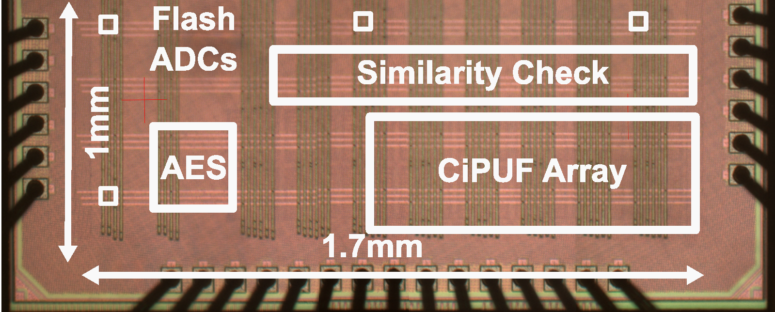
    Physical Unclonable Functions (PUFs) and Federated Learning (FL)

  • Explainability icon

    Explainable/Trustworthy Design

    Circuit design for explainable AI on Bio-medical Devices and Autonomous Driving

  • dice icon

    Stochastic Computation

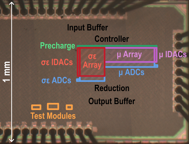
    Compute in Entropy (CIE): Utilize process variation for high energy-efficient computation

  • risc-v icon

    RISC-V

    Lightweigh RV32I RISC-V core for chip testing
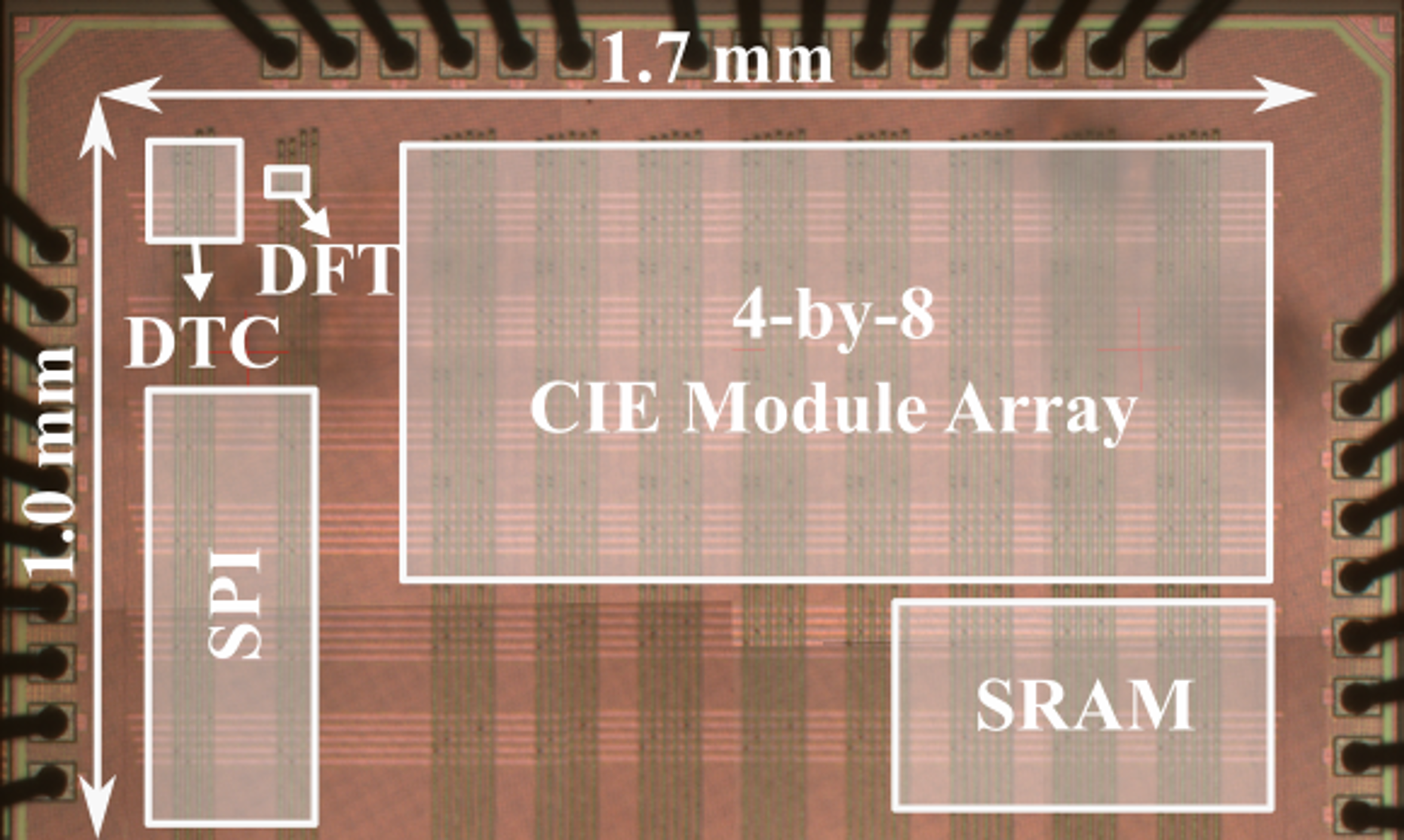
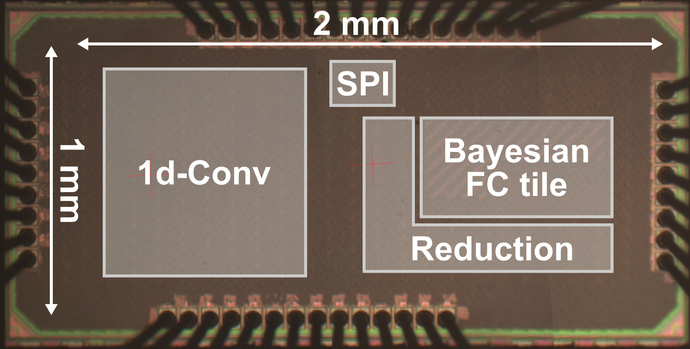
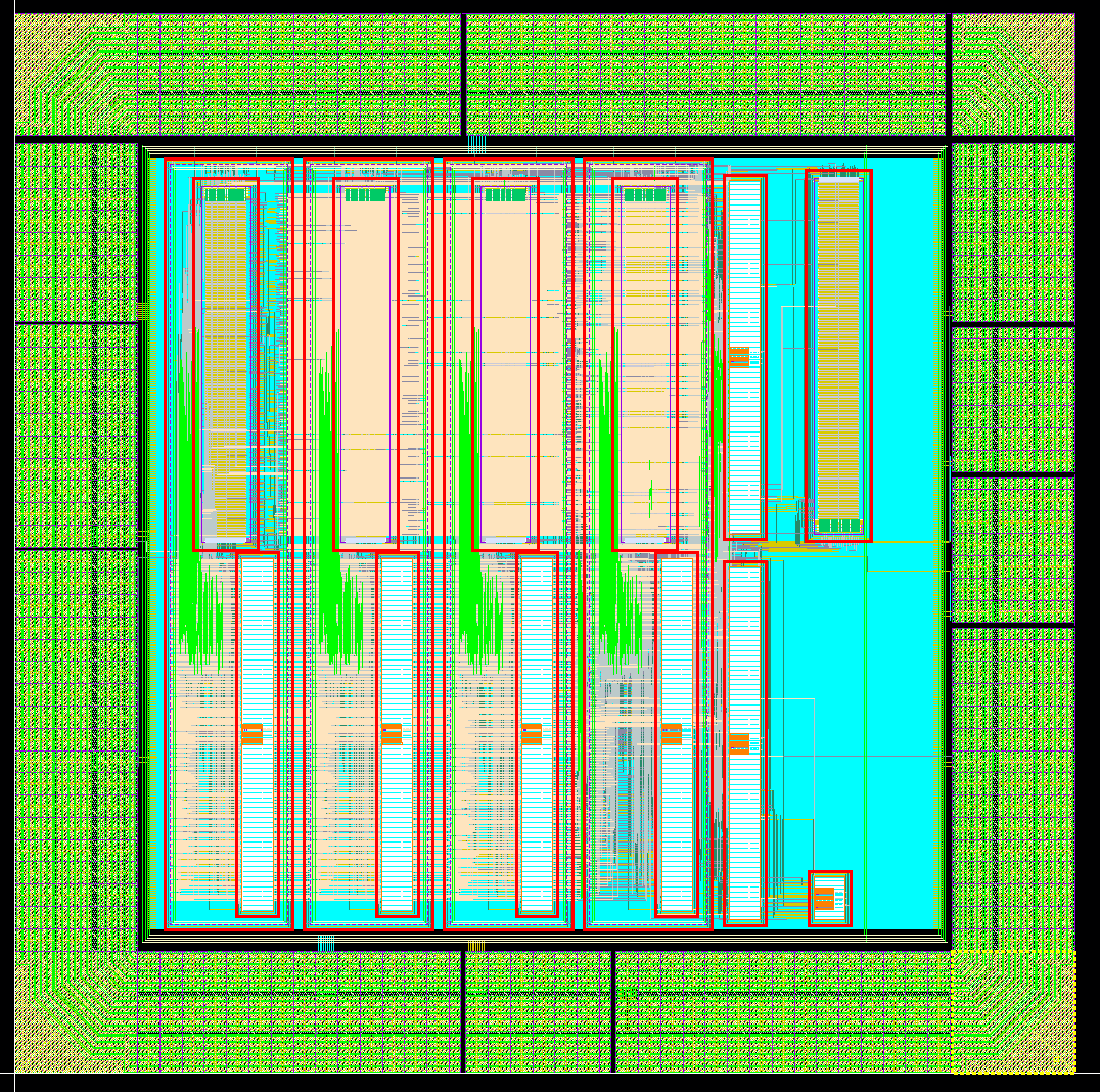
Chip Gallery

Resume

Education

  1. Ph.D.

    University of Notre Dame, Notre Dame, IN, USA

    Jan 2022 — present

    Department of Electrical Engineering

    Advisor: Prof. Ningyuan Cao

  2. M.S.

    University of Notre Dame, Notre Dame, IN, USA

    Jan 2022 — Jan 2026

    Department of Electrical Engineering

    Advisor: Prof. Ningyuan Cao

  3. B.S.

    Southeast University, Nanjing, Jiangsu, China

    Aug 2016 — Jun 2020

    School of Electronic Science and Engineering

Experience

  1. Internship

    Logic Pathfinding Lab Research Scientist - DTCO

    May 2025 — Aug 2025

    Samsung Semiconductor, San Jose, CA, USA (On-site)

    Design-Technology Co-Optimization (DTCO) Engineer at Samsung, focusing on advanced standard cell library and SRAM design. Experienced in developing DRC/LVS rule decks, and optimizing library architectures for diverse applications.

  2. Internship

    Logic Pathfinding Lab Research Scientist - SRAM

    May 2024 — Aug 2024

    Samsung Semiconductor, San Jose, CA, USA (On-site)

    Advanced Design of SRAM Bitcells and Peripheral Circuits

  3. Full-time

    Research Assistant

    Aug 2020 — Dec 2021

    Southeast University, Nanjing, Jiangsu, China (On-site)

    Advisor: Prof. Weiwei Shan

    Low-power digital IC design and fault-tolerant computing, developing energy-efficient and reliable computing architectures.

Download My PDF Resume
Open My Google Scholar

Publications

    Open My Google Scholar